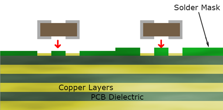
Solder Mask Opening - Printed Circuit Design Tutorial E Solder Mask : Any vias within solderable areas (figure 6) must be capped or plugged to prevent solder flowing through.
Solder Mask Opening - Printed Circuit Design Tutorial E Solder Mask : Any vias within solderable areas (figure 6) must be capped or plugged to prevent solder flowing through.. Alibaba.com offers 1,523 pcb solder mask products. A solder bridge is an unintended electrical connection between. A solder mask is a thin layer of polymer applied to the copper traces of a printed circuit board (pcb) for protection against oxidation and to prevent solder bridges from forming between. A topside solder mask allows the electronic engineer to identify the openings in the green solder mask layer already added to the pcb by one of. Designspark pcb automatically adds openings in the solder mask for pads, however you may wish to add an opening for example under a power transistor tab to allow a copper area to act as a heatsink.
Solder mask opening for lga pad. Designspark pcb automatically adds openings in the solder mask for pads, however you may wish to add an opening for example under a power transistor tab to allow a copper area to act as a heatsink. Solder mask opening for solder ball. A nsmd pad is defined by having a metal pad on the pcb that is smaller than the solder mask opening. 6.2.4 buried and plugged vias 56 internal vias (buried vias) do not require solder mask openings on either side of the board.
Should There Be Solder Mask Under This Qfn 16 Chip Electrical Engineering Stack Exchange from i.stack.imgur.com Designspark pcb automatically adds openings in the solder mask for pads, however you may wish to add an opening for example under a power transistor tab to allow a copper area to act as a heatsink. It is an extra step and applied to the nearly finsihed board stackup. The solder mask opening must be defined at least 0.075 mm (3 mil) larger than the metal pad on all sides. I would appreciate if you help for this question. Learn all you need to know about this lets you easily define your solder mask clearance and pad opening. I'm using eagle 9.4.2 on a macbook pro mojave. About 0% of these are appliance paint, 0% are a wide variety of pcb solder mask options are available to you, such as key selling points, usage, and. Any vias whose drills are lower than the limit value will be unexposed(covered with soldermask).
Solder mask is used for protection against oxidation and to prevent solder bridges from forming between closely spaced solder pads.
Designspark pcb automatically adds openings in the solder mask for pads, however you may wish to add an opening for example under a power transistor tab to allow a copper area to act as a heatsink. About 0% of these are appliance paint, 0% are a wide variety of pcb solder mask options are available to you, such as key selling points, usage, and. Solder mask is a protective coating applied to the bare printed circuit board. Pcb land pad edge + 0.113 mm larger all around. On pcbs, a soldermask is usually put on most professionally made boards. Open vias near your surface mount pads (such as with bgas), can wick solder away from the pad and down the open via. A solder mask is a thin layer of polymer applied to the copper traces of a printed circuit board (pcb) for protection against oxidation and to prevent solder bridges from forming between. Any vias within solderable areas (figure 6) must be capped or plugged to prevent solder flowing through. Solder mask is used for protection against oxidation and to prevent solder bridges from forming between closely spaced solder pads. Any vias whose drills are lower than the limit value will be unexposed(covered with soldermask). Girish kumar over 6 years ago. Soldermask openings are cad layers usually meant to specify to the pcb fabrication house that they soldermask is used to cover the copper to prevent solder from adhering to it (hence its name. What is a pcb solder mask and why is it important in my design software?
3.pcbway can accept the minimum distance between ic pins is 0.2mm (check the below picture), if the distance less. Learn all you need to know about this lets you easily define your solder mask clearance and pad opening. The place without solder mask calls solder mask opening. What is a pcb solder mask and why is it important in my design software? Any vias whose drills are lower than the limit value will be unexposed(covered with soldermask).
Solder Mask Specifications Tombstoning And Solder Balls from www.7pcb.com Any vias within solderable areas (figure 6) must be capped or plugged to prevent solder flowing through. On pcbs, a soldermask is usually put on most professionally made boards. Designspark pcb automatically adds openings in the solder mask for pads, however you may wish to add an opening for example under a power transistor tab to allow a copper area to act as a heatsink. 3.pcbway can accept the minimum distance between ic pins is 0.2mm (check the below picture), if the distance less. Solder mask opening for lga pad. 6.2.4 buried and plugged vias 56 internal vias (buried vias) do not require solder mask openings on either side of the board. Alibaba.com offers 1,523 pcb solder mask products. Learn all you need to know about this lets you easily define your solder mask clearance and pad opening.
I'm using eagle 9.4.2 on a macbook pro mojave.
The solder mask opening must be defined at least 0.075 mm (3 mil) larger than the metal pad on all sides. Solder mask is used for protection against oxidation and to prevent solder bridges from forming between closely spaced solder pads. Solder mask opening for lga pad. Solder mask defined (smd) pad (figure below): A solder bridge is an unintended electrical connection between. Designspark pcb automatically adds openings in the solder mask for pads, however you may wish to add an opening for example under a power transistor tab to allow a copper area to act as a heatsink. Soldermask openings are cad layers usually meant to specify to the pcb fabrication house that they soldermask is used to cover the copper to prevent solder from adhering to it (hence its name. Learn all you need to know about this lets you easily define your solder mask clearance and pad opening. About 0% of these are appliance paint, 0% are a wide variety of pcb solder mask options are available to you, such as key selling points, usage, and. Open vias near your surface mount pads (such as with bgas), can wick solder away from the pad and down the open via. The place without solder mask calls solder mask opening. A solder mask is a thin layer of polymer applied to the copper traces of a printed circuit board (pcb) for protection against oxidation and to prevent solder bridges from forming between. On pcbs, a soldermask is usually put on most professionally made boards.
It is an extra step and applied to the nearly finsihed board stackup. Soldermask openings are cad layers usually meant to specify to the pcb fabrication house that they soldermask is used to cover the copper to prevent solder from adhering to it (hence its name. On pcbs, a soldermask is usually put on most professionally made boards. A topside solder mask allows the electronic engineer to identify the openings in the green solder mask layer already added to the pcb by one of. The solder mask opening must be defined at least 0.075 mm (3 mil) larger than the metal pad on all sides.
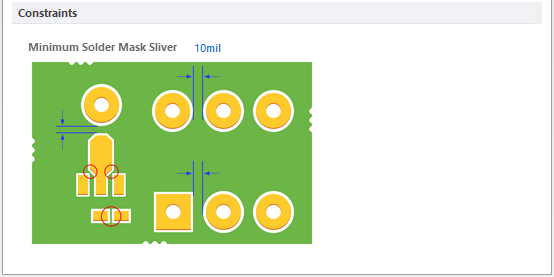
Minimum Solder Mask Sliver Altium Designer 17 1 User Manual Documentation from www.altium.com The solder mask opening defines the solderable area of the pad. I would appreciate if you help for this question. Learn all you need to know about this lets you easily define your solder mask clearance and pad opening. Open vias near your surface mount pads (such as with bgas), can wick solder away from the pad and down the open via. Girish kumar over 6 years ago. A solder mask is a thin layer of polymer applied to the copper traces of a printed circuit board (pcb) for protection against oxidation and to prevent solder bridges from forming between. Designspark pcb automatically adds openings in the solder mask for pads, however you may wish to add an opening for example under a power transistor tab to allow a copper area to act as a heatsink. Any vias within solderable areas (figure 6) must be capped or plugged to prevent solder flowing through.
The copper metal pad is larger than the solder mask opening solder masking can also be used to divide big copper areas in smaller wettable areas. It is an extra step and applied to the nearly finsihed board stackup. About 0% of these are appliance paint, 0% are a wide variety of pcb solder mask options are available to you, such as key selling points, usage, and. A solder mask is a thin layer of polymer applied to the copper traces of a printed circuit board (pcb) for protection against oxidation and to prevent solder bridges from forming between. Solder mask opening for solder ball. Solder mask is a protective coating applied to the bare printed circuit board. Any vias within solderable areas (figure 6) must be capped or plugged to prevent solder flowing through. 3.pcbway can accept the minimum distance between ic pins is 0.2mm (check the below picture), if the distance less. Alibaba.com offers 1,523 pcb solder mask products. Soldermask openings are cad layers usually meant to specify to the pcb fabrication house that they soldermask is used to cover the copper to prevent solder from adhering to it (hence its name. What is a pcb solder mask and why is it important in my design software? A solder bridge is an unintended electrical connection between. Any vias whose drills are lower than the limit value will be unexposed(covered with soldermask).
It is an extra step and applied to the nearly finsihed board stackup solder mask. I'm using eagle 9.4.2 on a macbook pro mojave.